中文ENGLISH
搜 索
琪埔维半导体,信立诚科技,华大半导体,航天民芯,Chipways,核芯互联,荣湃半导体,彭湃微,芯旺微,灵矽微,码灵微,沁恒微,芯昇科技,茂睿芯,微传,深圳市信立诚科技有限公司
24小时服务热线

15361428851

  • 首 页
  • 关于我们

    关于我们代理品牌荣誉资质

  • 产品中心

    ADC\DAC模拟芯片车规级芯片产品线ST兼容单片机单片机MCU传感器运放电源芯片存储芯片以太网芯片多串电池模拟前端AFE隔离器芯片DSP处理器芯片接口芯片射频芯片MOS管安全加密芯片蓝牙马达驱动高低边驱动时钟发生器时钟驱动通信模块方案产品

  • 品牌中心

    车规产品Chipways航天民芯核芯互联芯昇科技澎湃微华大半导体Chipon微传传感器希荻微沁恒微华芯微特奇力微聚洵半导体荣湃半导体澜智集成Techcode茂睿芯曦华科技优势分销品牌

  • 公司新闻
  • 行业资讯
  • 应用方案

    GTF192电子指纹锁方案电机FOC方案电子烟方案指纹模方案扫地机方案方案开发板芯片解决方案BLDC电机方案BMS锂电池管理方案

  • 下载中心

    产品规格书数据手册应用资料方案资料产品选型手册华大半导体资料下载

  • 样品申请
  • 联系我们

产品中心

ADC\DAC模拟芯片
车规级芯片产品线
ST兼容单片机
单片机MCU
传感器
运放
电源芯片
存储芯片
  • SPI NOR Flash
  • SPI NAND Flash
  • eMMC
  • DDR4
  • DDR3
  • SD NAND
  • EEPROM
以太网芯片
多串电池模拟前端AFE
隔离器芯片
DSP处理器芯片
接口芯片
射频芯片
MOS管
安全加密芯片
蓝牙
马达驱动高低边驱动
时钟发生器
时钟驱动
通信模块
方案产品

存储芯片

您现在的位置:首 页 > 产品中心 > 存储芯片 > DDR3

ZDV4128M16A-14DPH 2Gb

The 1Gb Double-Data-Rate-3 (DDR3(L)) DRAM is a high-speed CMOS SDRAM. It is internally configured as
an octal-bank DRAM. 
The 1Gb chip is organized as 8Mbit x16 I/O x 8 banks. These synchronous devices achieve high speed 
double-data-rate transfer rates of up to 2133 Mb/sec/pin for general applications. 
The chip is designed to comply with all key DDR3(L) DRAM key features and all of the control and address
inputs are synchronized with a pair of externally supplied differential clocks. Inputs are latched at the cross 
point of differential clocks (CK rising and CK
____
 falling). All I/Os are synchronized with a single ended DQS or
differential DQS pair in a source synchronous fashion. 
These devices operate with a single 1.5V ± 0.075V or 1.35V -0.067V/+0.1V power supply and are available in
BGA packages.


1GBIT DDR3 DRAM
VDD=VDDQ=1.5V(1.425V~1.575V)
VDD=VDDQ=1.35V(1.28V~1.45V),backward
compatible to 1.5V applications.
 8 banks
 8n-bit prefetch architecture
 Fully differential clock inputs (CK,CK) operation
 Bi-directional differential data strobe (DQS,DQS )
 On chip DLL align DQ, DQS and DQS
transition
With CK transition
 DM masks write data-in at the both rising and
falling edges of the data strobe
 All addresses and control inputs except data, data
strobes and data masks latched on the rising
edges of the clock
 Programmable CAS latency 5, 6, 7, 8, 9, 10, 11, 12,
13, 14 supported
 Programmable additive latency 0, CL-1, and CL-2
supported
 Programmable CAS Write latency (CWL) = 5, 6, 7,
8, 9, 10
 Programmable burst length 4/8 with both nibble
sequential and interleave mode
 BL switch on the fly
 Driver strength selected by MRS
 Dynamic On Die Termination
 Asynchronous RESET pin
 Internal (self) calibration: Internal self calibration
through ZQ pin (RZQ: 240 ohm ± 1%)
 TDQS (Termination Data Strobe) supported (x8
only)
 Write leveling
 Self refresh temperature (SRT)
 Automatic self refresh (ASR)
 JEDEC standard package
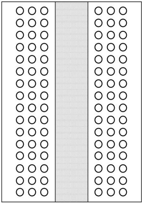
- 96ball FBGA(x16)
 Lead free & RoHS compliant
 JEDEC compliant
 Operating Temperature (Tcase)
- Commercial -C (0°C ≤ TC ≤ 95°C)
- Industrial -I (-40°C ≤ TC ≤ 95°C)

上一个:没有了

下一个:ZDV4128M16A-14IPH 2Gb

返回列表
友情链接:样品购买淘宝商城|航天民芯|琪埔维|澎湃微|

联系我们

深圳市信立诚科技有限公司

24小时服务热线:15361428851何生;18923860386莫先生

13410664847何生

开发板样品购买

客服热线

15361428851

客服邮箱在线客服

扫描关注信立诚微信

扫描关注信立诚微博

Copyright © 2018 Adobe. All rights reserved.隐私 使用条款 Cookie 京 ICP 备 10217899 号 京公网安备 110105010404

BACK THE TOP

  • 在线客服